Understanding Digital Logic Circuits Through Hands Circuit Diagram Module 1 introduces the basic building blocks of logic design. Module 2 introduces circuits that remember and store information. The Setup. The setup features a programmable microcontroller unit (MCU) with an onboard Custom Logic Block (CLB) module and a supporting MCU that sets the inputs and reads the outputs of the programmable MCU. The A programmable logic device (PLD) is an electronic component that can be configured to perform a specific logic function by the user. Unlike fixed logic devices that have predefined functions, such as logic gates or flip-flops, PLDs can be programmed and reprogrammed to implement different logic circuits. PLDs are widely…

Programmable logic. Logic gates are formed by connecting transistors together on a semiconductor material to make an integrated circuit. The wafers, or chips, of semiconductor contain lots of logic gates that make up different types of devices which work together to read, store, calculate, and transmit digital information. •A simple programmable logic device (SPLD) is a programmable logic device with complexity below that of a complex programmable logic device (CPLD). •Simple combinational PLDs are capable of realizing from 2 to 10 functions of 4 to 16 variables with a single integrated circuit. •The PLDs such as PLAs, PALs are simple PLDs.
Programmable Logic Devices Circuit Diagram
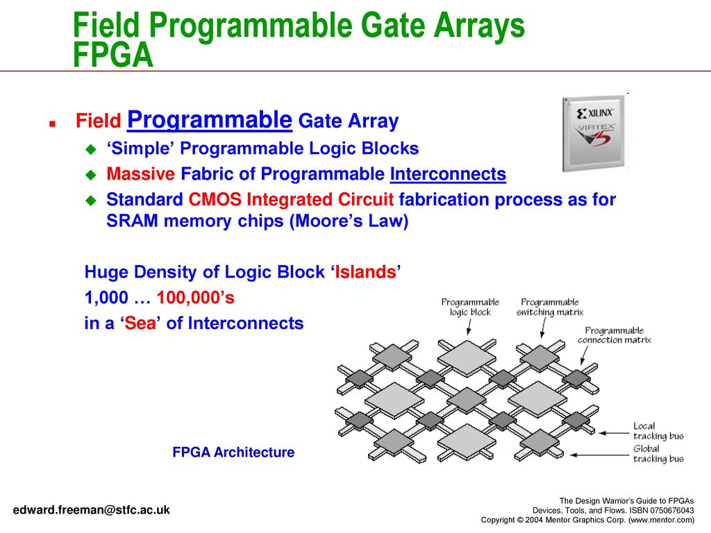
The complex programmable logic device (CPLD) such as the XC2C32A from Xilinx, and the field programmable gate array (FPGA) such as the XC3S50 from Xilinx are some of the newer versions of programmable logic that are a result of improvements to the original types of devices.
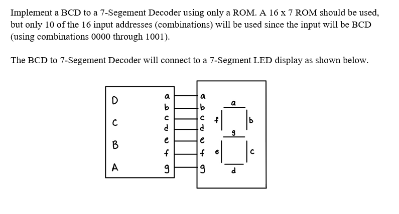
A Programmable Logic Array (PLA) is the implementation of the combinational logic circuits using a programmable type of a digital logic device. There is a programmable AND gate array with a programmable OR gate inputted thereafter, a feature that enables users to specify the required custom logic.
PDF Combinational Logic Design with Verilog Circuit Diagram
advanced programmable logic software, you will find this book an interesting insight into a different way to design. Programmable logic devices were invented in the late seventies and since then have proved to be very popular and are now one of the largest growing sectors in the semiconductor industry. Why are programmable logic devices so
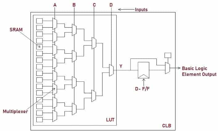
January 30, 2012 ECE 152A - Digital Design Principles 4 Programmable Logic Provides low cost and flexibility in a design Replace multiple discrete gates with single device Logical design can be changed by reprogramming the device No change in board design Logical design can be changed even after the part has been soldered onto the circuit board in ¾ How to implement digital circuits using PLAs and PALs. Introduction: An IC that contains large numbers of gates, flip-flops, etc. that can be configured by the user to perform different functions is called a Programmable Logic Device (PLD). The internal logic gates and/or connections of PLDs can be changed/configured by a programming process.
